The board has two large chips on it: a Zynq UltraScale+ RFSoC and a Kintex UltraScale FPGA beside it, joined by eight high-speed serial lanes. Neither chip is big enough on its own for everything we wanted to run. So the plan was to make the second chip an extension of the first: a place to push extra logic, plus the block of memory sitting right next to it, all reachable across the link. An AI did the work under the Python2Verilog framework; I set the direction at a few key points.
This post is about how that second chip became compute and memory for the first, and about the one beat in the middle where every simulation passed and the hardware still did nothing.
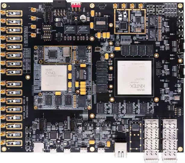
Two chips, one seam
The two chips are joined only by those eight serial lanes. Everything the first chip wants from the second - run a module over there, read a value out of the far memory - has to travel that seam and come back. So the whole design reduces to one question: is the seam honest? If a byte that goes out comes back changed, nothing built on top of it can be trusted.
The link itself is one we wrote, kept deliberately thin. The vendor’s own link block did not work out on this board, so instead of leaning on a heavy protocol we made our own and let it stay simple. It carries framed messages, and the very first piece of each message says what it is. Some are memory requests: read or write the second chip’s memory. Some are control messages, right down to rebooting the far chip over the same link, with no cable to reach for. And some are just raw data for the decoder - there is no separate “run compute” command at all, because the decoder sits right in the path, so a message arriving simply is its input. Thin link, and the first thing in each message decides what happens.
We settled that the only way that counts: on the real hardware, against a reference, byte for byte. Not a simulation that agrees with itself, but the actual chips, checked against a known-good answer.
Three jobs, each checked on real hardware
By the end the second chip was doing three distinct jobs for the first, and each was proven the same way - on the board, not in simulation, against a known answer:
- A round-trip data test. Data went across the link to the second chip and came back. It matched byte for byte.
- A decoder running remotely. A decoder sat on the second chip, took its soft input across the link, did the work, and handed the hard result back. It matched the reference model with zero errors - and did it twice in a row, with no reset in between, to prove it re-arms on its own.
- Remote memory, read back. A value written into the far memory and read back came out exactly as written, at one address and then at another deep in the range.
That is what “extension” means here. The second chip is a pipe, a place to compute, and a block of memory, and all three are trustworthy for the same reason: each was checked against a reference on the hardware itself, not on a model that could quietly agree with a mistake.
The beat where everything lied
Getting there was not smooth, and the middle of it is worth telling because the lesson outlived the board.
One direction of the link would not come up. The receiver watches for a run of well-formed markers and, once it sees enough of them in a row, declares itself locked. One direction locked at once. The other never did.
So we chased it, and every check came back clean. The vendor’s own example locked in simulation. A loopback matched a frame exactly. A cross-chip simulation wired to the real connections locked both directions and matched byte for byte. A post-layout comparison of the working and broken builds came back identical. The physical signal was pristine. Every layer had been checked and cleared, and the hardware stayed exactly as broken as before.
Every one of those checks was a statistic - a lock, a pass, a percentage - and a statistic hides what the signal actually is. So the AI grabbed a few raw words straight off the wire while the link claimed to be locked. They were a plain repeating pattern: a bare clock, a square wave, with no data riding on it at all.
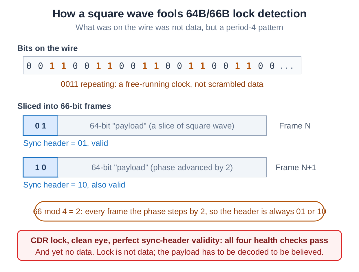
The coincidence that made this so convincing is small and mean. Sliced into frames, a pure clock pattern lands its two-bit header on a legal value every time. So it satisfies the lock detector, satisfies the eye check, satisfies the validity meter - and carries no information whatsoever. A meaningless repeating pattern was impersonating a healthy link.
If the wire carries a free-running clock, nothing is driving it. So the AI measured the lane connections directly, trusting only the physical names printed on both chips, not the tool’s internal numbering, and sending a distinct coded marker down each lane so it could tell them apart. The result was the exact reverse of the record everyone had been trusting.
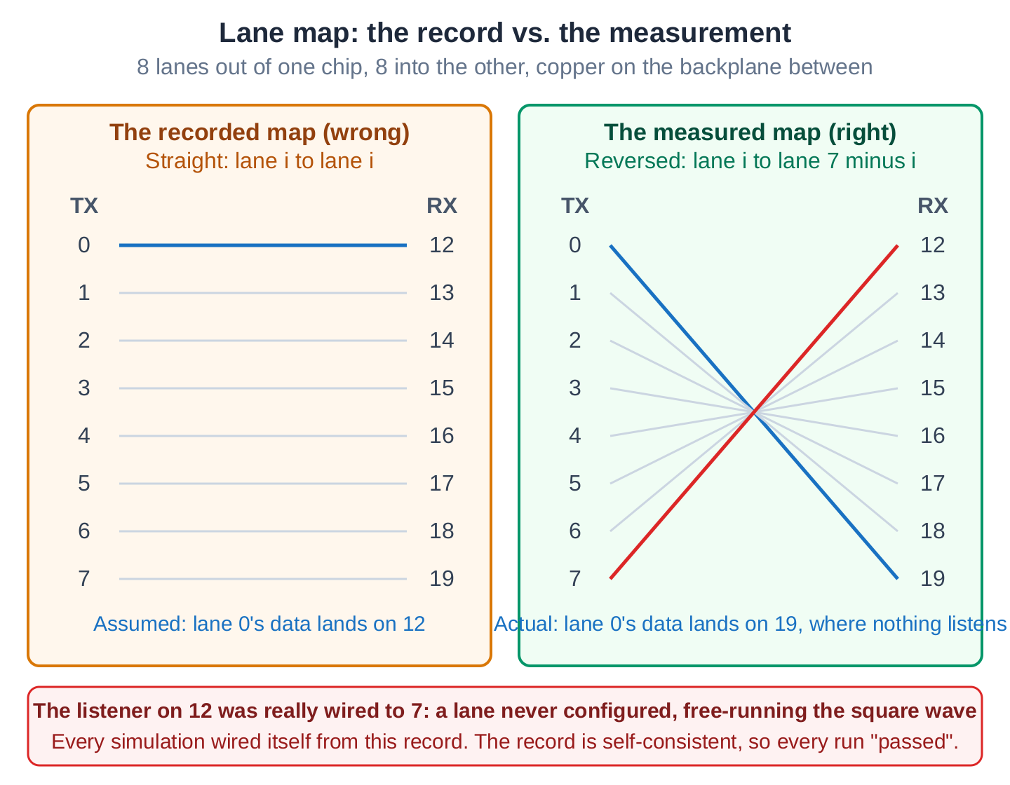
There was the trap. The transmitter really was sending correct data - to a lane nobody was listening on. The input everyone watched was wired to a lane that had never been configured, so it oscillated on its own. Every simulation had drawn its wiring from that same record. The record was internally consistent, so every simulation reproduced the same wrong connection and passed. Layer after layer of verification agreed with each other because they all read from one shared, wrong assumption.
The uncomfortable detail: the record even carried a note saying it had been verified on silicon. The note was real; the verification behind it was the accidental lock of the very first lane. The answer had been sitting on the schematic the whole time. Pointed at the two correct lanes, the link came up on the first try and matched byte for byte.
And the reversal was not just a note written backwards. It is baked into the board itself: the lanes between the two chips are wired in reversed order in the copper, and that cannot be changed. This is the real reason the vendor’s ready-made link was never going to work here. It insists that both chips agree on the order of the lanes before it will combine them, so with the order reversed in the copper, it could never lock. That is why we wrote our own thin link in the first place: it does not try to combine the lanes that way, so it simply does not care that their order is reversed.
What survives this
When every layer of the circuit checks out and the hardware still does nothing, the thing left to doubt is the measurement itself. That backwards record survived a full day of work for one reason: every simulation was faithfully obeying it. The circuit was never lying. The map was.
Trust the hardware over the document that describes it. Read a connection by its physical name, not a number in a table. And do not call a link proven until you have decoded a real payload off it and checked it byte for byte - a lock, an eye, a passing meter can all be satisfied by a signal that carries nothing.
With the seam honest, the rest fell into place, and the second chip took its place as compute and memory for the first: one board, two FPGAs, and a link you can actually trust.
Notes
- Hardware: a custom board pairing an AMD Zynq UltraScale+ RFSoC (XCZU67DR) with an AMD Kintex UltraScale FPGA (XCKU115), joined by eight high-speed serial lanes.
- The link, remote-compute, and remote-memory logic, and all of the debugging, were done by an AI under the Python2Verilog framework. Everything cited was read on the board or matched against a reference in the same session.
- This is a follow-on to “Bringing Up Linux on an RFSoC Board in a Day”.