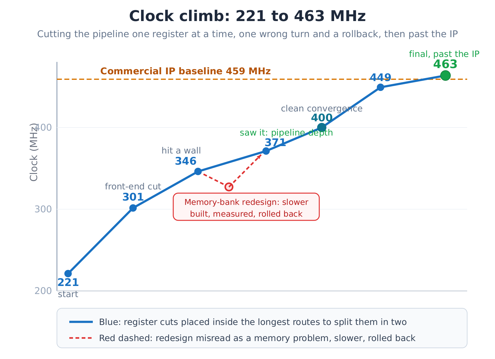
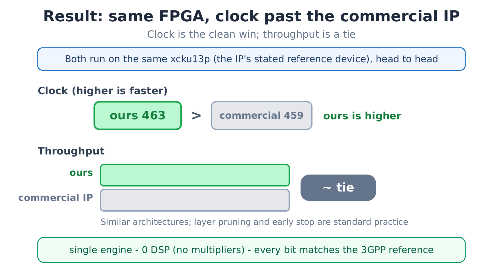
Getting a model to write a few lines of code is no longer remarkable. The harder thing is to take a real RTL design and optimize it to its physical limit, without breaking a single bit. This is a case study of exactly that: a 5G LDPC decoder, generated as Verilog from a Python algorithm, then handed to an AI to close timing. It started at 221 MHz, hit a wall, took one wrong turn, and finished at 463 MHz - past the 459 MHz a paid commercial IP reaches on the very same FPGA.
The interesting part is not that an AI wrote the code. It is that it could read the physical constraints, tell the right fix from the wrong one, back out of a dead end, and finally chew through the one obstacle that runs through every LDPC decoder: the data dependency between layers. That is where it starts to behave like an engineer.
Why raising the clock is not simple
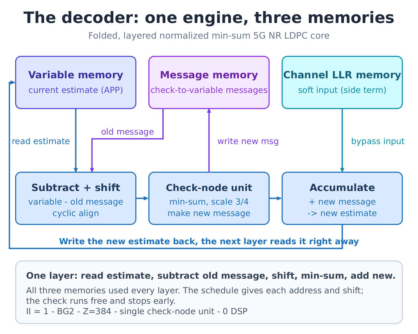
On an FPGA the decoder is a loop: read each bit’s current estimate, subtract the old message and cyclically shift, let the check-node unit compute new messages, then accumulate those with the channel information and write back. The estimates, messages, and channel values live in three separate memories, used on every layer, iterating layer after layer until the codeword is self-consistent and an early stop fires.
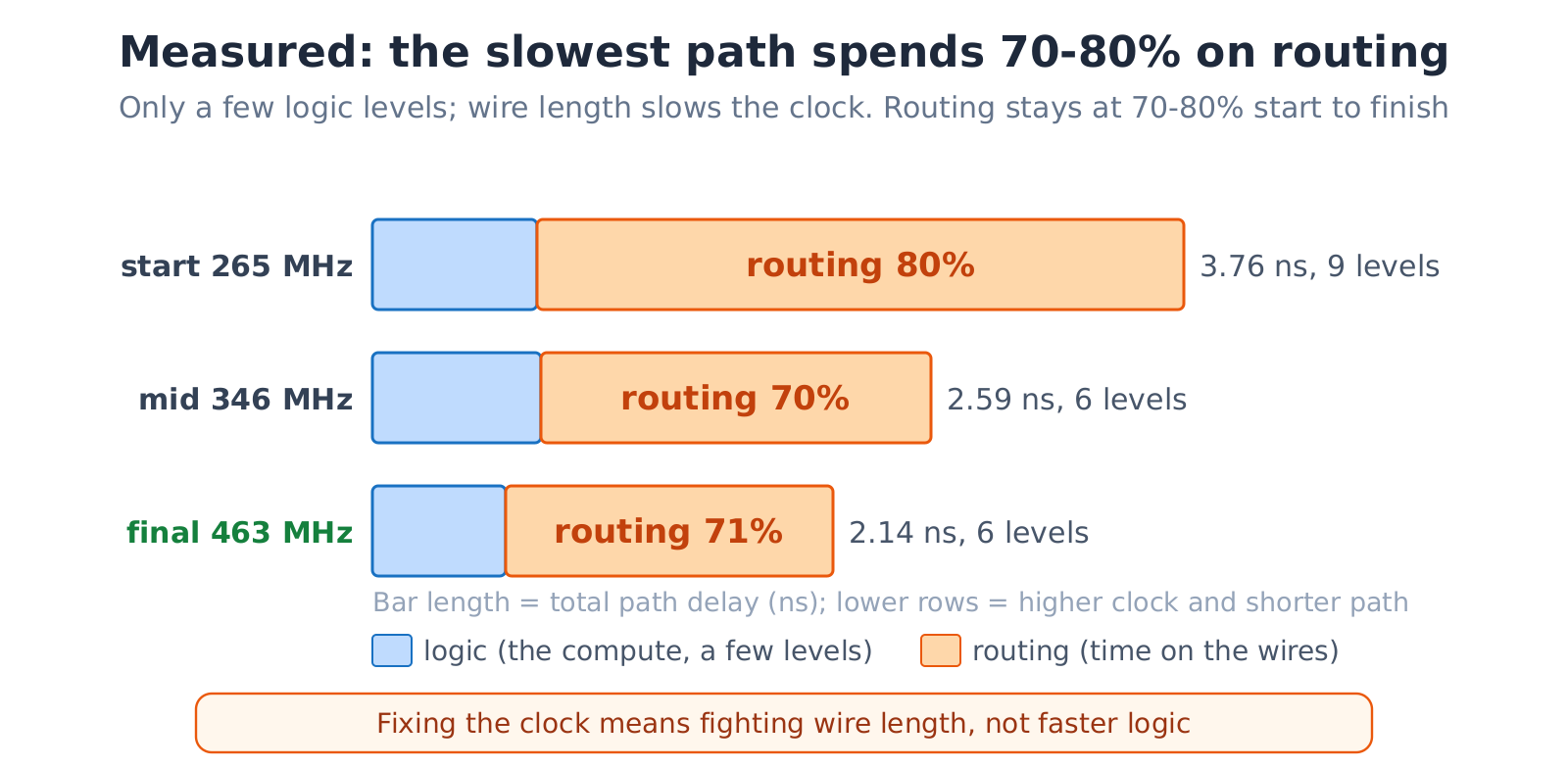
A higher clock processes more data per second, so it is one of the central goals. But each cycle, a signal has to leave one register, pass through a few levels of logic, travel along real physical wiring, and reach the next register within a single clock period. If even one such path does not finish in time, that critical path holds the whole chip’s clock back. And on a modern FPGA, the slowest path is usually dominated by wiring, not logic. At the finish line, the slowest path here totals about 2.1 ns - the logic that actually computes takes only a fraction of that, and roughly seventy percent of the time is spent in routing.
Whether a slow path is logic-bound or routing-bound decides which fix to reach for. The direct fix for a long wire is to insert a register in the middle, splitting one long segment into two short ones that each finish within a cycle. The register has to land in the middle of the long wire; putting it at either end is wasted.
The real obstacle: the dependency between layers
Picture the variable memory as a shared scratchpad holding every bit’s best guess. Each layer reads it, runs one round of checks, and writes back - and the very next layer immediately reads that just-updated scratchpad. That write-then-read dependency is what makes inserting a register dangerous here: the register delays the update by a cycle, the next layer reads on its old schedule, gets a stale value, and the decode diverges.
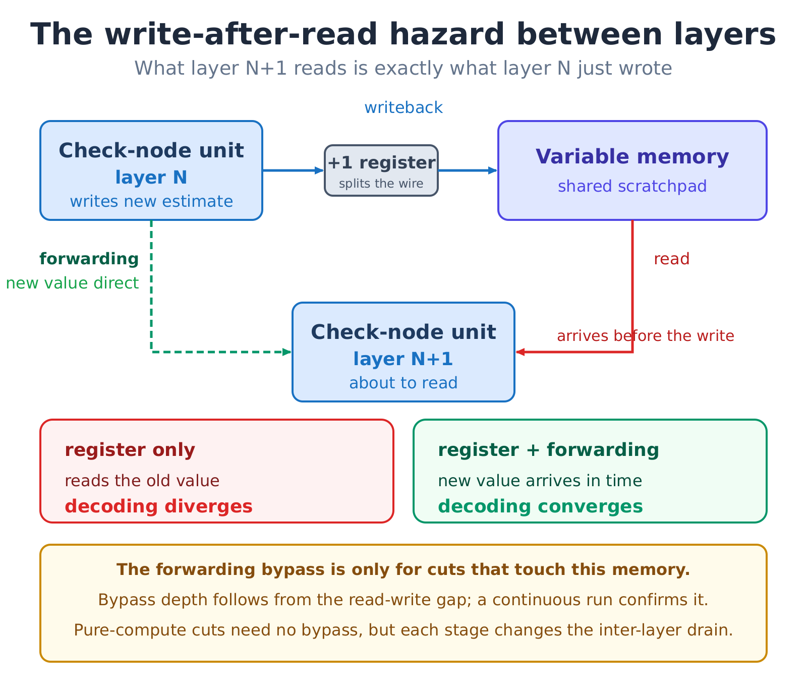
It is also sneaky: the first test frame is often green, because the scratchpad starts at zero and the stale value happens to be zero too; only continuous decoding exposes it. So any cut that touches the shared memory needs a forwarding bypass alongside it, sized just deep enough to never read stale.
A wrong turn: blaming the memory
After hitting a wall, the AI suspected the memory structure itself was the ceiling, and proposed an ambitious fix: split the large memories into smaller banks so compute and storage sit closer together. This was not just talk - it was implemented, synthesized, and placed and routed. The result was a cold shower: the rebuild did not speed anything up; the extra addressing and boundary logic made the clock slightly slower, and the change was rolled back.
The valuable part was the post-mortem. Reading the real report for that slowest path showed it was never a memory-addressing path at all - it was a compute-and-fetch path, already packed tightly into one corner of the chip. The problem was never how the memory was arranged; it was that this compute path was not pipelined deeply enough.
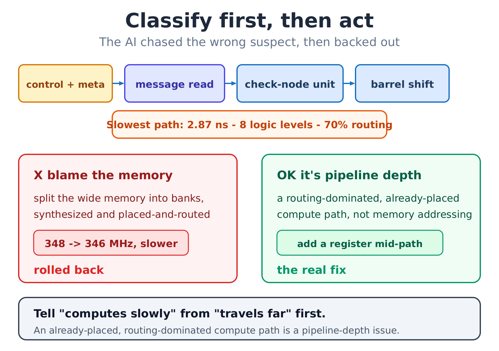
The lesson is the expensive kind: before rebuilding a large block, pull out the current slowest path and classify it as logic-bound or routing-bound. Effort spent on the wrong diagnosis only makes things worse.
Six cuts, past 459 MHz
Once the path was correctly read as a pipeline-depth problem, the way forward opened up. The AI returned to the plain method - insert registers into the middle of the slowest compute-and-fetch wires, with a forwarding bypass wherever a cut touched memory - now placed more precisely. A few representative moves: register the read port of a memory to shorten the path after it without changing read timing; register the write stage to give data an extra cycle to reach memory; or relocate an existing midpoint register for a free gain at no added latency. Six cuts took the clock from the mid-300s to 463 MHz, converging cleanly along the way and crossing the commercial IP’s 459.
Two side notes. One was a false alarm about congestion - the report showed none, just a few similar-length paths stuck together. The other was a counter-intuitive result about over-constraining: usually setting the clock target too high makes the tool give up, but this design had placement headroom, so a tighter target actually forced a better outcome. Rules of thumb have conditions; applied blindly they backfire.
What about throughput? A tie
To be honest, throughput did not win. The two architectures are similar and finished roughly even, edging ahead only because of the slightly higher clock. At this code rate both grind only the layers that actually carry information, and early stopping is standard practice on both sides. The one clean win here is the clock.
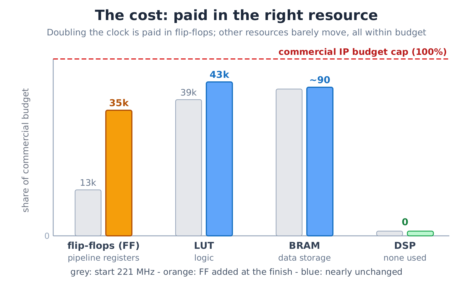
The cost: paid in the cheapest resource
Doubling the clock costs something; what matters is which resource pays. The registers and bypasses added along the way are spent almost entirely in flip-flops, while the lookup tables and block RAM barely moved and DSP usage stayed at zero. Through every step, all resources stayed inside the commercial IP’s budget. Flip-flops are the cheapest, most plentiful resource on an FPGA, so spending the cost there is a good trade.
Every cut still matches the reference
Speed is worthless if a bit is wrong, so one rule held throughout: after every change, the hardware output was checked bit-for-bit against the algorithm reference in simulation, with no bit allowed to differ. The finished decoder was cross-validated against the 3GPP implementation in the MATLAB 5G Toolbox - the encode side matched bit-for-bit across many random trials, and the decode side matched the official implementation in full across several channel configurations.
What I took away
More portable than the number are a few judgments this path kept proving. Classify before you act: tell a slow path’s cause before choosing a fix - effort on the wrong diagnosis only makes things worse. Do not fear admitting a wrong turn: the memory rebuild was built, measured, slower, reverted, and accepting a clean negative result is itself engineering. The hardest part is usually the dependency you cannot route around. And compare honestly: the clock genuinely won, the throughput tied, and saying so is what earns a reader’s trust.
Have you ever been certain the bottleneck was in one place, fought it for hours, and found you had been looking at the wrong thing the whole time?