The board has two large chips on it. A Zynq UltraScale+ RFSoC runs Linux and holds everything, and a Kintex UltraScale sits beside it, joined by a high-speed serial link. In the last post that second chip became an extension of the first: a place to run logic, and a block of memory reachable across the link.
One cable was still in the way. An FPGA keeps its logic in volatile memory, so it forgets everything the moment power drops. Reloading it meant reaching for a programming cable from a workstation, every single time. Fast link, real compute, and a wire hanging off the board.
This post is about taking that wire out: sending the firmware over the same link the data uses, writing it into the memory chip beside the target, and then telling the target to restart itself from it. An AI did the hands-on work under the Python2Verilog framework; I set the direction at a few points, and flipped one switch with my own finger.
Why the obvious path does not work
There have always been two ways to get logic into an FPGA. Push it straight into the chip’s configuration memory and it takes effect immediately, but that memory is volatile and the image is gone at the next power-off. Or write it into the flash memory chip sitting next to the FPGA, which the chip reads by itself every time it powers up. Debugging always used the first, over the cable.
The first path cannot ride the link, and the reason is worth sitting with for a second. Loading the configuration memory rewrites the whole chip, and the logic carrying the link is part of that chip. Half way through the transfer, the thing carrying the transfer stops existing. Writing the flash and then rebooting is the standard route for a remote update, and it is the one we built.
A memory channel hiding inside the data stream
The flash chip beside the second FPGA is 64 megabytes and sits on the dedicated configuration pins. Those pins have a property that makes this whole thing cheap: once a design is running, it can keep reaching them through an internal port, so the flash costs no ordinary pins at all.
So the link protocol grew one more message type. Frames whose header carries a tag divert into a flash channel; everything else passes through as data, untouched. Behind the tag sits a controller that talks to the flash on its own free-running clock, which matters more than it sounds: erasing a sector takes far longer than a link hiccup, and a controller clocked off the link would abandon an erase half-finished. Bulk work moves 128 kilobytes per round trip.
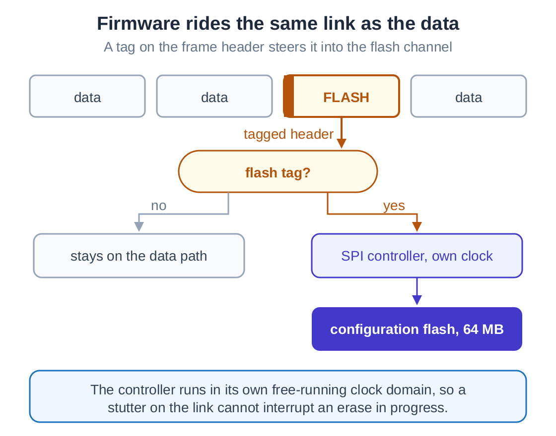
The flash command set stayed on the host side, deliberately. The logic on the FPGA knows no vendor opcodes at all, it just moves bytes, which means the same channel works against a different flash chip on a different board without touching the hardware.
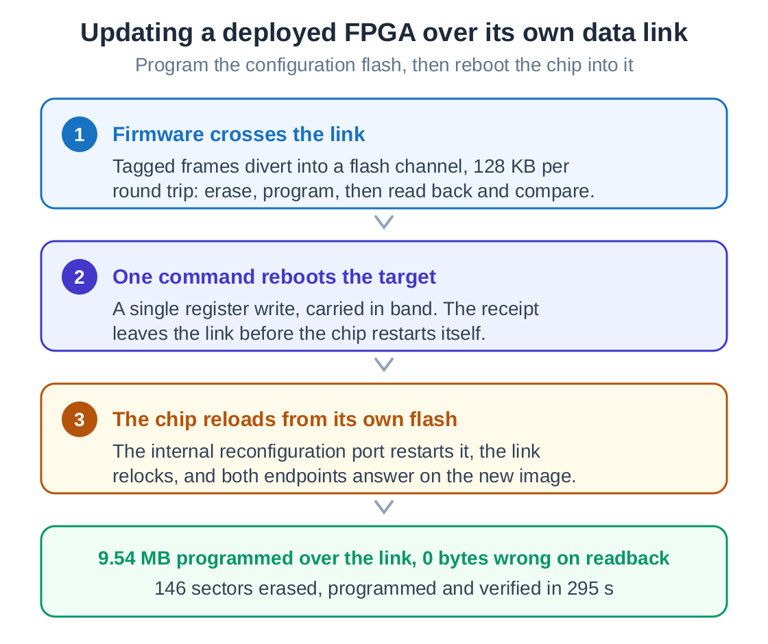
Three checks on the real board. The device identifier read back over the link matched the exact part printed on the schematic. A single-sector test at a high address erased, wrote, read back and erased again, byte for byte. Then the whole thing: 8.56 megabytes written at address zero and read back in 165 seconds with not one byte different.
The write path worked. A complete firmware image was sitting in the flash. All that remained was to make the chip read it at power-up.
The boot test said no, and the register said nothing
Where an FPGA looks for its image at power-up is set by three mode pins on the package. The schematic printed a default, and the default meant flash boot. So we commanded a reconfigure from those pins, and the chip went dark. Nothing loaded.
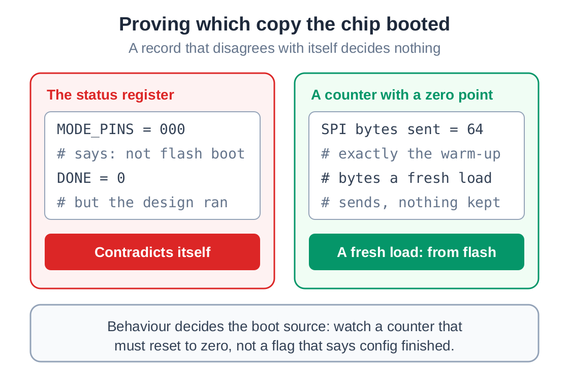
Reading the configuration status register was the obvious next move. It reported the mode pins as 000, which is not flash boot. It also reported that configuration had never finished, on a design that was visibly running and answering our messages over the link at that exact moment.
That second reading is the interesting one. A register that contradicts itself is not weak evidence, it is no evidence. Whatever path produced that readback was broken, so nothing it says about the mode pins can be trusted either. The lesson from the previous post applied again: records lie, behavior does not. The reconfigure attempt had already given the honest answer.
Back to the drawing, then, and the same trick as last time: extract the schematic geometrically and pull out that corner of the circuit. The three mode pins land on a four-position DIP switch, and the default printed in the corner of the drawing had never been set on the assembled board. The setting we wanted differed from the assembled one in exactly one bit, so one position had to move. Which direction means “on” did not matter, because flipping is flipping either way.
Proving which copy it booted
One switch flip later, the chip configured itself. But “configuration finished” is a weak claim. It does not distinguish between the chip loading the flash copy and the chip still running an older image the cable had left behind.
The design has a counter that records how many bytes the flash interface has sent. It read 64: exactly the warm-up bytes a fresh load sends, and not one more. That counter cannot survive a reload, so the only way to read 64 is to have started from nothing. That is what named the boot source, and no status flag could have.
Then the cable came off entirely. One register write sent over the link, with the acknowledgement leaving the link before the chip restarted, so that a silent failure could never look like a silent success. The chip reloaded itself from flash through its internal reconfiguration port, the link relocked a few seconds later, and both endpoints answered on the new image.
From that point on, changing the second chip’s firmware is a remote update. The host writes the new image into the flash, sends one command, and the chip comes back on it. Pull the power and it still comes back on it.
The same flow, on a wider link
We later ran the whole thing again on a wider path: two lanes bonded together, with the datapath inside the chip widened so the bonded capacity could actually be used. The same loopback test went from 3.0 to 5.24 gigabits per second, and the link’s own ceiling moved far enough that the limit now sits inside the chip rather than on the wire.
Over that bonded path the full update ran end to end: 9.54 megabytes, 146 sectors erased, programmed and verified with no byte different, in 295 seconds, followed by a remote reboot with every check answering on the first read. Programming and rebooting now run on a system that programmed itself.
Three rules I kept
Each of these went back into the framework as a check that runs on every build.
Trust behavior, not records. A status register read from a running design reported two things that cannot both be true. Command the action for real and let the hardware answer.
Send the receipt before the action. A command that ends in a reboot loses its own reply, so success and failure look identical from the host. The acknowledgement leaves first, then the chip restarts.
A boot-source proof needs a zero point. To know which image a chip is running, watch a counter that must reset on a fresh load. Whether configuration reported success says nothing about where the image came from.
The previous post ended by saying that wiring is now something we measure rather than assume. This one says the same about booting. The drawing claimed one setting, the register claimed another, and neither counted. What counted was the moment the chip actually came up on its own flash.
The only job left on that cable is live debugging, and there is a standard way to carry that over a network too. Once it moves onto this link, the wire is done.